It’s time to think about closed loop control. The control loops exists mostly in software, but uses values scaled and shifted in hardware to minimise the error – in this post I describe how it all fits together. I’m not planning a particularly complicated feedback scheme – PI or PID should be enough. The part that did require extensive thinking, was to keep track of the different units in the system and managing all this within the constraints of an 8 bit micro.

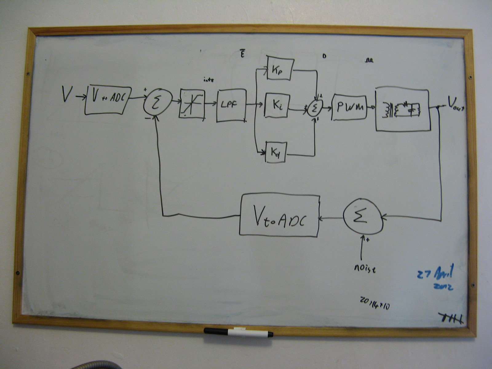
Starting on the left, the user specifies a target voltage V. This is converted to a target ADC value by the VtoADC function. This gives the setpoint for the control loop – we will try to get the feedback ADC value to match the target ADC value. The actual ADC value is subtracted from the setpoint to give the error that we are trying to minimise.
I first limit the size of the error to fit in an 8 bit value (i.e. between -128 and 127), then this value goes into the low-pass filter. By restricting the magnitude of the error, I only have to store 8-bit values in my filter, thus conserving precious RAM. This also limits the rate of change of the output voltage, which dampens overshoot by slowing down the control loop. I found that adjusting the output too quickly can cause the host computer to detect a short circuit – limiting the magnitude here helps to avoid that problem.
The output of the low-pass filter (vaguely labeled ε here) now represents a smoothed error term. This goes into the PID section of the loop, to find the desired duty cycle (D) for the PWM module. Note that I’m currently only using the proportional term of the PID controller, with the other terms set to 0. When the rest of the circuit stabilises, I’ll improve the controller response by tuning these.
Here we cross from software into hardware. The duty cycle value determines the shape of the PWM wave, which in turn drives the MOSFET to switch the current in the transformer. On the secondary side of the transformer, after the rectifying diode and output filters, we find the output voltage.
However, this voltage is determined by the load resistance, so we have to measure the voltage and return a value to the primary side. We can measure the voltage connecting the output to the optocoupler diode through a resistor. Back on the primary side, the diode current flows through a resistor to generate a voltage. This voltage is in turn measured by the AVR’s ADC. This complicated is a fairly complicated conversion from out voltage to ADC value – I represent it in the lower block labeled VtoADC. The original VtoADC function (top left) converts the desired input voltage to the ADC setpoint by mimicking this hardware conversion – just how well it can replicate it will determine how accurately the setpoint voltage can be tracked. Finally, it is likely that the measured value will contain some noise too, so that adds into the control loop just before conversion.
We can track this feedback value back around the control loop now: an error is calculated, then filtered, and the used result to adjust the PWM duty cycle according to the PID controller. And that is closed loop control.
Another constraint, which is not shown on this diagram, is that the PWM duty cycle is also limited. This limits the average of power delivered to the transformer to safe levels (<2.5W), and also limits the peak transformer current to stay within the allowed range.
Note the five scratches in the lower righthand corner – I’m counting the number of times I’ve managed to crash my laptop.
