This blog has moved. You can now find me here.
USB current meter

Specifications:
- > 600mA measurement range
- <10mA resolution
- <5% error
- Power switch
- Warning LED at 400mA
White
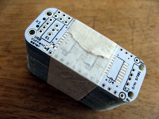
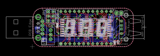
Another month, another board version. This time the updated edition of the USB current meter. And not just one, but 20 boards; kindly made by Seeed Studios. White (of course!), with rounded corners, about the size of a USB drive. Once assembled, it is pleasingly solid to hold. These boards are meant to serve as demonstration samples: I can populate them, show them to people, and mail them all over the world. In addition, building more than one unit adds confidence that the circuit functions as expected.
The only major change on this revision is the use of an ZXCT1010 to measure the output current – my previous LM358-based effort struggled at low currents, and required a larger sense voltage than I felt comfortable with. The ZXCT1010 is suitably sensitive, highly linear and requires very little additional components. (I did, however, spend a day debugging an unexpectedly high transimpedance, before I realised that I had been referring to the datasheet of the ZXCT1110.)
In addition to the change in current sensing, I moved the components closer together and shortened the board to be less than 50mm long. The LED also moved to be next to the switch. Although the footprint for the programming header is still present, I plan on leaving it unpopulated, and just connecting using pogo pins.
A circular dependency?
v0.2 bringup
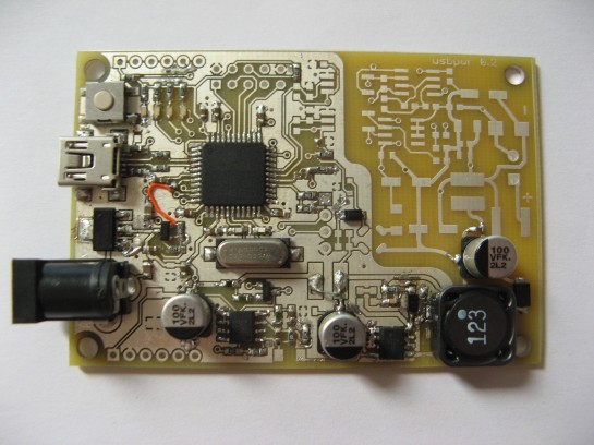
I’ve started soldering the v0.2 board, testing and porting the v0.1 software as I go along. The LED, button, and ADC channels all moved, which required adjustment of a couple of header files. Two minor wire mods were required, but so far everything tested is working. There is a tiny bit of coupling between the PWM signal and the ADC feedback signal, but I suspect a well placed capacitor will clean the line up.
From here, I have to do the following:
- Populate the auxiliary transformer and generate a sane voltage rail for the opamps on the secondary side.
- Populate the feedback circuitry.
- Adjust the ADC driver to use the new configuration.
- Calibrate.
And then I can test my primary side current monitoring.
Current monitor
My boards arrived from PCBtrain a few weeks ago, so you’d expect enthusiastic assembly to ensue. However, most of my time is going into finding a job, so I’ve made relatively little progress. I started with the current monitor, to see what it feels like when assembled – so far I’m very happy. It’s just like a slightly heavier memory stick.
The ATtiny does what it should, the LCD can display what I tell it to, and the switch works fine too. Currently I’m recalculating the resistor values for current measurement, as I seem to have made the gain optimistically small. A similar measurement circuit is used in the power supply, so this provides a clean space to make sure it words exactly as designed.
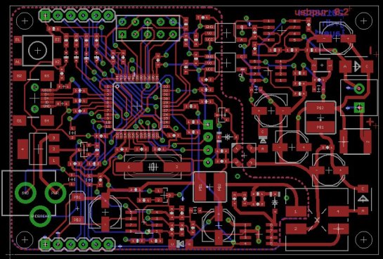
Layout rev 0.2
Layout for rev 0.2 is complete, it’s PCBtrain time again. I should get the boards before the bank holiday season starts next week.
Key changes to rev 0.2:
- Improved voltage and current monitoring on the isolated side
- Fixed Atmega PWM pin.
- Improved filtering on voltage rails – there is space for play here, with an excessive number of cap footprints.
- Different inductor – higher peak current, smaller package, lower price. Also lower isolation.
- Size is now 75mm x 50mm (was 60mm x 50mm)
Blog is live
It’s time to face the world. I’m making the blog live, so you can see posts collected over the last few months, with some more recent but back-dated ones too.
USB current monitor
The power supply is meant to be a tool. But to build a tool, you need tools. And sometimes you need to build those too.
Measuring the efficiency of the power supply is hard. I can measure the output voltage over a known resistance, and calculate the output power. But at the moment I have no input power measurements, except if I run it from a bench power supply. And the bench supply goes through an LDO, so I have to compensate for that too. Initially, I assumed that my laptop would complain around 2.5W, so I turned up the output until the USB voltage dropped, and calculated the efficiency as quite high. However, with more tuning of the PWM frequency, I managed to get the measured output power to 2.7W. Apparently my laptop is quite forgiving if you increase the power demand very slowly. But this means I need a better tool.
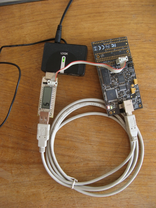
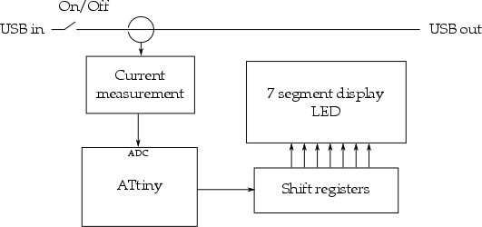
One option is to cut open a USB cable and connect a ammeter in series. A more procrastinatory option, however, is to build a dedicated USB current monitor. You simply plug it in, it measures the current passing through, and displays it. A warning LED for high currents. So that’s where my weekend went.
This is a quite a simple circuit, so I won’t go into too much detail. The current measurement is done with an LM358 measuring the voltage drop over a low-side sense resistor. This is scaled to an appropriate level for the ATtiny’s ADC (i.e. < 2.5V). The ATtiny doesn’t have enough pins to drive a cheap display, so I use three bytes worth of shift register to control the 7-segment LCD.
Why an ATtiny? Price, mostly. They are small, relatively cheap, and allows reuse of code written for the power supply.
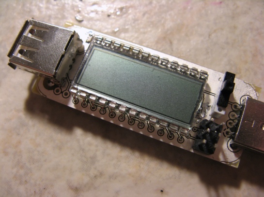
After layout, the board is about the size of a USB flash drive, most of it filled by the 3 digit LCD. I’ll piggyback it on my next manufacturing order, then I can write some code.
Closing the loop
It’s time to think about closed loop control. The control loops exists mostly in software, but uses values scaled and shifted in hardware to minimise the error – in this post I describe how it all fits together. I’m not planning a particularly complicated feedback scheme – PI or PID should be enough. The part that did require extensive thinking, was to keep track of the different units in the system and managing all this within the constraints of an 8 bit micro.
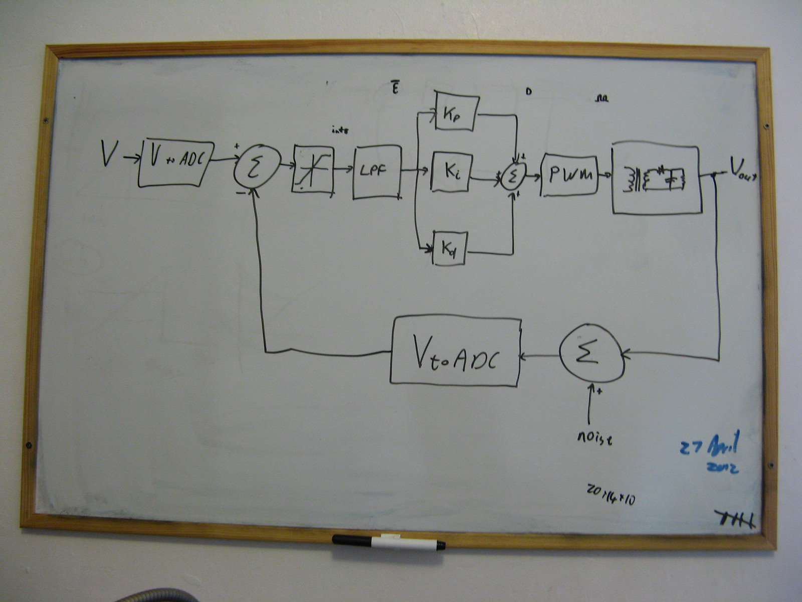
Starting on the left, the user specifies a target voltage V. This is converted to a target ADC value by the VtoADC function. This gives the setpoint for the control loop – we will try to get the feedback ADC value to match the target ADC value. The actual ADC value is subtracted from the setpoint to give the error that we are trying to minimise.
I first limit the size of the error to fit in an 8 bit value (i.e. between -128 and 127), then this value goes into the low-pass filter. By restricting the magnitude of the error, I only have to store 8-bit values in my filter, thus conserving precious RAM. This also limits the rate of change of the output voltage, which dampens overshoot by slowing down the control loop. I found that adjusting the output too quickly can cause the host computer to detect a short circuit – limiting the magnitude here helps to avoid that problem.
The output of the low-pass filter (vaguely labeled ε here) now represents a smoothed error term. This goes into the PID section of the loop, to find the desired duty cycle (D) for the PWM module. Note that I’m currently only using the proportional term of the PID controller, with the other terms set to 0. When the rest of the circuit stabilises, I’ll improve the controller response by tuning these.
Here we cross from software into hardware. The duty cycle value determines the shape of the PWM wave, which in turn drives the MOSFET to switch the current in the transformer. On the secondary side of the transformer, after the rectifying diode and output filters, we find the output voltage.
However, this voltage is determined by the load resistance, so we have to measure the voltage and return a value to the primary side. We can measure the voltage connecting the output to the optocoupler diode through a resistor. Back on the primary side, the diode current flows through a resistor to generate a voltage. This voltage is in turn measured by the AVR’s ADC. This complicated is a fairly complicated conversion from out voltage to ADC value – I represent it in the lower block labeled VtoADC. The original VtoADC function (top left) converts the desired input voltage to the ADC setpoint by mimicking this hardware conversion – just how well it can replicate it will determine how accurately the setpoint voltage can be tracked. Finally, it is likely that the measured value will contain some noise too, so that adds into the control loop just before conversion.
We can track this feedback value back around the control loop now: an error is calculated, then filtered, and the used result to adjust the PWM duty cycle according to the PID controller. And that is closed loop control.
Another constraint, which is not shown on this diagram, is that the PWM duty cycle is also limited. This limits the average of power delivered to the transformer to safe levels (<2.5W), and also limits the peak transformer current to stay within the allowed range.
Note the five scratches in the lower righthand corner – I’m counting the number of times I’ve managed to crash my laptop.
